After some discussion within the team, we have finished the design work of the PCB.
The next 2 pictures shows the preview of the PCB.
Overview
Let’s take a closer look at the details.
The boxes represents the various sections of the PCB. They are numbered anti-clockwise from the top left.
1: Analog to Digital Converter (ADC)
This section consists of the ADC itself, a 24 bit Microchip Tech part, and a 2.048V voltage reference.
2: Air pressure, humidity and temperature sensor
Sensor onboard is a BME280
3: Analog Power Regulator
We will take a closer look at the power supply considerations later.
4: User Button
5: GPS header
GPS is connected to UART 1 of the ESP32
6: Micro SD Card
SD Card is connected to SDIO of the ESP32. Propagation delay of the traces are matched to within 25ps of each other.
(Probably an overkill but why not?)
7: Main Power Regulator
8: On Board Programmer
9A: ESP32, a WiFi and Bluetooth capable module
9B: Antenna for ESP32
The antenna is designed to hang outside of the board for optimal performance.
Power
Power is supplied from a 6-12V source – a 2s LiPo or even single lead acid battery.
A DC-DC buck converter was used for high efficiency.
In order to provide smooth power for the devices on board, 2 sets of low dropout linear regulators (LDO) are used.
The 2 LDO supply analog and digital power as shown in the above diagram.
Analog and digital power are supplied separately in order to prevent fast switching digital circuits from introducing noise in the analog circuits.
ADC
The ADC, Microchip MCP3561 , has 8 differential inputs – 4 channels.
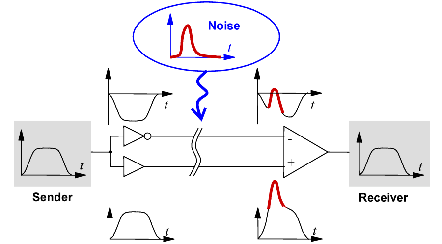
In a differential signal, the wire pairs are twisted, hence any noise introduced will be introduce into both of of the individual wires.
By measuring the voltage difference in the pair, any noise introduce is effectively cancelled out.

Image by courtesy of Altium (https://www.altium.com/documentation/altium-designer/differential-pair-routing-ad)
Supporting the ADC is a Microchip MCP1501T, generating a 2.048V voltage reference for the conversion.
The MCP1501T was chosen for it’s stability over a wide range of temperature and it’s regulation capabilities (this is a topic I will not go into).
Temperature, Humidity and Pressure Sensor
BME280 was chosen for as it is integrated (3 in 1), speaks both I2C and SPI, and has a library written for it.
Since this is an analog sensor (with a digital interface), the BME280 is powered from the analog supply.
Analog Power Design
Layer 3 of PCB, showing the analog power plane
In order to maintain extremely low noise in the analog supply, separate copper pours was used for both digital and analog supplies.
Care was taken such that any analog or digital signal does not cross out of it’s own power plane. (with the exception of channel 4)
ESP32
The ESP32-WROVER-IB is chosen as it has the option for an external antenna through it’s IPX (1st gen) connector.
A small section of the PCB is cut out for the antenna of the ESP32. This ensures that the tuning of the antenna is unaffected and the antenna can radiate properly without any obstacles. This ensure that the tuning of the antenna is not affected by the PCB.
Conclusion
The above is a summary of the main considerations in the design and layout of the PCB. Much time was spent selecting parts, discussing what is important and what is feasible. All while trying to keep within reasonable time and cost.
The design has been sent for fabrication on the 3rd of August. In the next post we will be taking a look at the assembled PCBs.


