Completed PCBs and Preliminary Tests

The PCB finally arrived earlier this week and the team has assembled a total of 5 boards. I opted to systematically hand solder the PCB first while individually testing various parts of it. By doing so, I was able to confirm the hardware works as expected and troubleshoot it easily. Here are the photos of the completed board.

Good news! All the individual component works as expected. (after some troubleshooting 😶)

The PCB was soldered and tested in the following order:

  1. Buck converter
  2. Digital 3.3V supply
  3. USB to UART converter and USB
  4. ESP32
  5. SD Card
  6. Analog 3.3V supply
  7. ADC and supporting components

Total time taken was roughly 6 hours.

Preliminary Tests

Let’s take a look at the performance of the hardware.

Power Supply

The power supply unit (PSU) on the right is feeding power into the main input of the PCB and the multimeter is measuring the output of the 5V buck converter. This shows that the buck converter is able to produce a 5V output (with a ~0.8% error) even when fed with 6V input.

Note that this test is conducted when the ESP32 is on idle, ie low load. This should be considered the absolute minimum voltage and not the operating voltage.

ADC

Next, we’ll take a look at the accuracy of the voltage reference.

The accuracy of the ADC is directly dependent on the accuracy and stability of the voltage reference.

The multimeter is measuring the output of the voltage reference after passing through a low pass filter (LPF). As shown, the voltage is spot on at 2.045V. As we currently do not have the capabilities to perform any form of noise measurements on the voltage reference. Also, we will skip the ADC performance test for now.

ESP32, USB and SD Card

Justin has written a test program to write a file into the SD card and read it back.

This ensures that:

  1. The USB to UART converter is working and is able to program the ESP32 with no issue
  2. The ESP32 is functional
  3. The SD card is functional

The SD card is mounted successfully, and read and write operations are successful.

BME280

Screenshot by courtesy of Justin.

As shown in the above screenshot, the ESP32 is able to read the temperature, pressure and humidity respectively.


Issues in Hardware

Hotplate process produced inconsistent results

After I hand soldered and confirmed that the PCB is indeed working, the team proceeded to use hotplate to reflow 4 other boards. There were however, different issues with different boards, with different ICs either not soldered on properly or has pins that were shorted together.

The team has concluded that this was due to the process not being optimised for reflowing. This could be due many factors such as, the kind of solder paste used, the thickness of the stencil, the size of the pads etc.

This required additional rework after the reflow process.

Programming of ESP32 with SDIO lines pulled up

IO2 of the EPS32 is a bootstrap pin, meaning that this has to left floating in order to go into programming mode…….. Only if you’re programming for the first time.

We noticed that some boards couldn’t be programmed. However, there wasn’t an issue with the schematics. Turns out desoldering the pullup resistor on IO2 before programming for the first time worked. Thereafter, the pullup resistor had to soldered back in, in order to use the SD card. We suspect this might be due to the ESP32 internal efuse not being programmed from the factory.

High Quiescent Current Draw

Quiescent current is the current that a device draws when it is in idle mode. In our case, with everything powered down, we have ~6mA current draw at 12V. That works out to be about 15mA at 5V. While the ESP32 is capable of very low power draw, down to 0.1mA in power saving mode, this would not matter if everything else on the board is drawing 15mA.

After some quick probing on the board, we have determined that the current draw comes from:

  1. Low Dropout Regulator (2x 5mA)
  2. LEDs (2x 2.5mA)

We have placed an order for new low quiescent current LDOs. However, for the next revision of hardware, low current draw will one of the main focus.

Missing USB power diode

During the process of PCB design a diode to provide provide to the board from USB was unintentionally left out, as a result, the board cannot be powered from USB. This was quickly solved by soldering a ‘botch’ wire from the USB connector to the 5V supply.


Next Steps

We will be looking at how we can optimise the current design over the one or two weeks. Stay tuned for more details!


Edit 22 Aug 2020

Issue with the Programming ESP32 with SDIO Lines Pulled Up

It appears that our conclusion that this issue only occurs when programming for the first time may not be entirely true. Some boards can’t be programmed with IO2 pulled up regardless it is the first time or not. This issue can be fixed be allowing the software to control the pull up. However, changes has to be made on the hardware.

One of the changes for the next revision, we will be connecting the pull up to the SD card power, rather than the main (always on) power.

PCB Status Update

After some discussion within the team, we have finished the design work of the PCB.

The next 2 pictures shows the preview of the PCB.

Overview

Let’s take a closer look at the details.

The boxes represents the various sections of the PCB. They are numbered anti-clockwise from the top left.

1: Analog to Digital Converter (ADC)

This section consists of the ADC itself, a 24 bit Microchip Tech part, and a 2.048V voltage reference.

2: Air pressure, humidity and temperature sensor

Sensor onboard is a BME280

3: Analog Power Regulator

We will take a closer look at the power supply considerations later.

4: User Button

5: GPS header

GPS is connected to UART 1 of the ESP32

6: Micro SD Card

SD Card is connected to SDIO of the ESP32. Propagation delay of the traces are matched to within 25ps of each other.

(Probably an overkill but why not?)

7: Main Power Regulator

8: On Board Programmer

9A: ESP32, a WiFi and Bluetooth capable module

9B: Antenna for ESP32

The antenna is designed to hang outside of the board for optimal performance.

Power

Power is supplied from a 6-12V source – a 2s LiPo or even single lead acid battery.

A DC-DC buck converter was used for high efficiency.

In order to provide smooth power for the devices on board, 2 sets of low dropout linear regulators (LDO) are used.

The 2 LDO supply analog and digital power as shown in the above diagram.

Analog and digital power are supplied separately in order to prevent fast switching digital circuits from introducing noise in the analog circuits.


ADC

The ADC, Microchip MCP3561 , has 8 differential inputs – 4 channels.

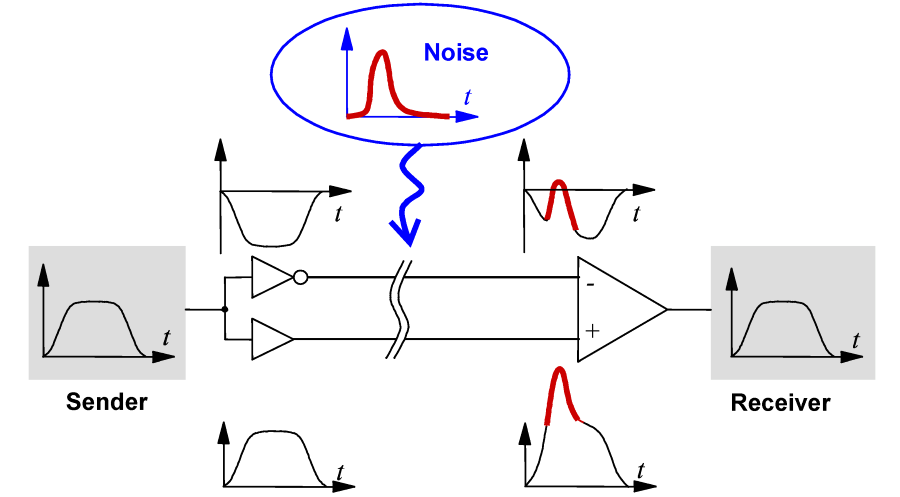
In a differential signal, the wire pairs are twisted, hence any noise introduced will be introduce into both of of the individual wires.

By measuring the voltage difference in the pair, any noise introduce is effectively cancelled out.

Explanatory diagram showing how differential signaling works

Image by courtesy of Altium (https://www.altium.com/documentation/altium-designer/differential-pair-routing-ad)

Supporting the ADC is a Microchip MCP1501T, generating a 2.048V voltage reference for the conversion.

The MCP1501T was chosen for it’s stability over a wide range of temperature and it’s regulation capabilities (this is a topic I will not go into).


Temperature, Humidity and Pressure Sensor

BME280 was chosen for as it is integrated (3 in 1), speaks both I2C and SPI, and has a library written for it.

Since this is an analog sensor (with a digital interface), the BME280 is powered from the analog supply.


Analog Power Design

Layer 3 of PCB, showing the analog power plane

In order to maintain extremely low noise in the analog supply, separate copper pours was used for both digital and analog supplies.

Care was taken such that any analog or digital signal does not cross out of it’s own power plane. (with the exception of channel 4)


ESP32

The ESP32-WROVER-IB is chosen as it has the option for an external antenna through it’s IPX (1st gen) connector.

A small section of the PCB is cut out for the antenna of the ESP32. This ensures that the tuning of the antenna is unaffected and the antenna can radiate properly without any obstacles. This ensure that the tuning of the antenna is not affected by the PCB.


Conclusion

The above is a summary of the main considerations in the design and layout of the PCB. Much time was spent selecting parts, discussing what is important and what is feasible. All while trying to keep within reasonable time and cost.

The design has been sent for fabrication on the 3rd of August. In the next post we will be taking a look at the assembled PCBs.

PCB Rev 3 Proposal

Following the previous electronics update, a few tradeoffs has to be made.

Battery Life

Taking measurements at high rates 100+sps requires the microcontroller (MCU) to be active most of the time. This has a large impact on the battery life of the device. For this reason, we will be using larger batteries which takes up more space. In addition, we will be using 18650 Li-Ion cells as they are more energy dense than the more common LiPo cells.

Size

The size of our datalogger will be relatively large, with the majority of the space taken up by the Li-Ion cells. As a result, we will not make an attempt to compact the PCB, and optimize for performance instead.

Instrumentation

Since we are moving towards research grade instrumentation, is more economical to have the sensor interface separate from the main MCU and data storage board. This allows us to design new interfaces for different sensors as needed without redesigning the costly MCU section.

Furthermore, this means that we can adapt the datalogger to accept any kind of sensors.

Proposal

Here we present the 3rd revision electronics.

As discussed, the PCB is broken into 2 parts – motherboard and daughterboard. 

At the heart of the motherboard is the ESP32, a MCU with a built-in WiFi transceiver. Stores data into a SD card and sends data over WiFi to the UAV as it flies past.

The purpose of the daughterboard is to power the various sensors and amplify the signal before sending it over to the Analog to Digital Converter (ADC) on the motherboard.

Analog signals are differential and sent over twisted pairs. This ensures that the signal is not affected by any nearby electromagnetic interference (EMI).

Lastly, the option of external power supply allows the operator to attach a high capacity battery (eg lead acid battery) for long term operation.

Printed Circuit Board (PCB) Rev 3

The original PCB was designed for low sample rate, long range transmission and long battery life.
However, these design goals have to change to accommodate for the new project specifications.

In this new PCB design revision, we will attempt to achieve:

  1. High Resolution (24 bits native, 22 bits effective)
  2. High Sampling Rate (<80sps)
  3. High Transmission Rate (noted in previous blog post)

Resolution

In order to achieve high resolution, the analog front end has to be carefully routed to reduce the effect of noise. For this reason, we will be using a differential Analog to Digital Converter (ADC). [Link to a paper by Microchip]

Sampling Rate

Sampling rate is limited by the speed of the ADC, data bus and internal storage medium. Sampling rates of more than 1ksps are possible, but we will be limited by the transmission rate as noted in the previous post.

Transmission Rate

Since LoRa was not designed for high transmission rate, we will be designing the new PCB around a WiFi transceiver, ESP32.

The Art of PCB Routing

When making analog or high speed designs, special care must be taken in order to reduce noise or error in the signals. There are a few things to take note of, such as isolated analog and digital planes, shielding nearby high speed digital traces etc.

We are definitely not experts in PCB layout and some research has to be done in this area. It is our goal to be able to achieve 22 effective bits of resolution or better.